— Laser Direct Writing —
- PCB Circuit Exposure
- PCB Solder Mask Exposure
- Broad Semiconductor Packaging

PCB Circuit Exposure
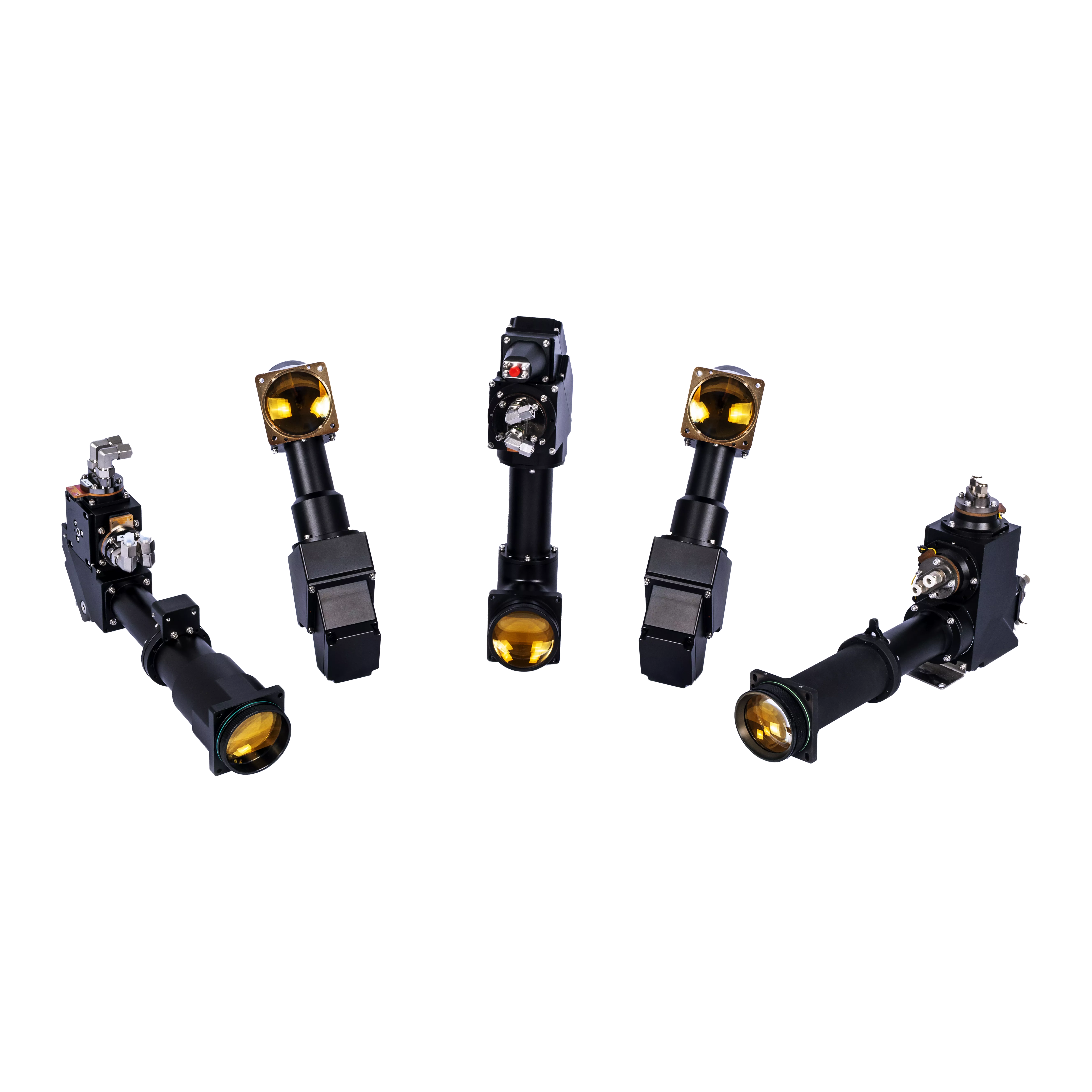
Laser direct lithography technology uses a laser beam to directly irradiate the substrate surface, forming nano-scale patterns on the target substrate in a single pass without the need for costly photomasks, resulting in a shorter production preparation cycle.
At present, this process technology has been widely used in PCB, advanced packaging, FPD (flat panel display) and photomask manufacturing.— Litronics Solutions —


Tel | 0512-68237866
Email | litronics@litronics.cn
Add | Room 401, 402, Building 1, Zone C, Science and Technology City Industrial Park, No. 588 Wutaishan Road, High-tech Zone, Suzhou
Working Hours | Monday–Friday 9:00–18:00